Shopping Cart
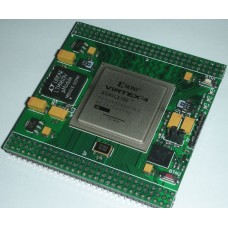
0 item(s) - 0.00€XMF4 XILINX FPGA MODULE
Add to Compare
Estimate shipping:
| * Country: | |
| * Region / State: | |
| * Post Code: |
XILINX VIRTEX-4 XMF4 FPGA module is designed for rapid prototyping and implementing FPGA designs. Board can be used for educational purposes. It can work independently, or can be used as control module in the bigger design.
Features
1) XILINX XC4VLX100 FPGA
• 110592 Logic Cells
• 96 XtremeDSP Slices
• 240x 18Kb RAM blocks (4320Kb, 500MHz)
• 12 Digital Clock Managers
• 768 User I/O (182 routed on this board)
2) XILINX XCF32P FLASH
• 32Mbit Platform Flash PROM
• IEEE Standard 1149.1/1532 Boundary-Scan (JTAG) support for programming
• Endurance of 20000 Program/Erase Cycles
3) Onboard IO peripherals
• 50MHz CMOS oscillator
• 4 LEDs
• 1 push button
4) Handy configuration
• Standard 2.54mm JTAG header
• Mode select jumper (JTAG or FLASH)
• DONE LED
• Push button for manual initiation of configuration process
• Reset supervision by voltage monitor
5) Onboard power supply
• 3.3V 4A (IO, PERIPHERALS)
• 2.5V 0.8A (VCCAUX)
• 1.2V 4A (CORE VOLTAGE)
• 1.8V 1A (Platform FLASH)
• Input voltage range 6V – 15V
• POWER-GOOD LED
• J6 and J7 jumpers to use external I/O voltage 1.14V-3.45V
6) 168 independent I/O routed to the connectors
• J4 3x29 male pin connector (84 IO, 3 GND)
• J5 3x29 male pin connector (84 IO, 3 VCC)
• 2.54mm pitch for all connectors
• 1.14V-3.45V External I/O voltage can be used
• 41 differential pairs
• Small 74x74mm PCB designed to fit on the prototyping board with 2.54mm pitch
| FPGA / CPLD | |
| Equivalent Logic Cells | XC4VSX55 - 55296 XC4VLX100 - 110592 XC4VLX160 - 152064 |
| Block RAM Bits | XC4VSX55 - 5760 XC4VLX100 - 4320 XC4VLX160 - 5184 |
| Digital Clock Managers | XC4VSX55 - 8 XC4VLX100 - 12 XC4VLX160 - 12 |
| Development board | |
| Crystal oscillator | 50 MHz CMOS |
| IO LEDs | 4 |
| IO push buttons | 1 |
| IO routed to connectors | 168 |
| FLASH | |
| Flash size | XC4VSX55 - 32 Mbit XC4VLX100 - 32 Mbit XC4VLX160 - 32 Mbit + 8 Mbit |
| Flash type | XILINX Platform Flash PROM |


