Shopping Cart
0 item(s) - 0.00€XMF5 XILINX FPGA MODULE
Add to Compare
Estimate shipping:
| * Country: | |
| * Region / State: | |
| * Post Code: |
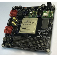
Xilinx Virtex-5 XMF5 FPGA module is designed for rapid prototyping and implementing FPGA projects. Module can be used for educational purposes. Module can work independently, or as control module in the bigger design.
Features
1) XILINX XC5VLX155T FFG1136 FPGA
• 24320 Virtex-5 Slices (155648 Logic Cells)
• 128 DSP48E Slices
• 212x 36Kb RAM blocks (7632Kb, 550MHz)
• 6 Clock Management Tiles
• 1 Endpoint Block for PCI Express
• 4 Ethernet MACs
• 16 GTP RocketIO 3.75 Gb/s Transceivers (6 routed on this board)
• 640 User I/O (211 routed on this board)
2) ST M25P64 SPI Flash
• 64Mbit
• SPI Bus Interface
• FPGA configuration
• Post-configuration access
• More than 100000 Program/Erase Cycles and 20-year data retention
3) Onboard IO peripherals
• 256Mbit 133MHz SDRAM
• 256Kbit EEPROM
• CH340G USB UART port
• 50MHz CMOS oscillator for IO
• 75MHz LVPECL oscillator for Rocket IO
• Four IO LEDs
• Two IO push buttons
4) RocketIO Transceivers
• 2x SATA HOST port
• 2x SATA TARGET port
• One MGT clock input routed to SMA connectors
• Two transceivers routed to 1.27mm male header
5) Handy configuration
• 14-pin JTAG header
• 14-pin SPI header
• Direct or Indirect Programming of SPI Flash
• Mode select jumper (JTAG or FLASH)
• Push button for manual initiation of the configuration process
• Header for external reset
• Reset supervision by the voltage monitor
• DONE LED
6) Onboard power supply
• 3.3V 3A (IO, PERIPHERALS)
• 2.5V 0.8A (VCCAUX)
• 1V 10A (CORE VOLTAGE)
• 1.2V 3A (Rocket IO)
• Input voltage range 4.5V – 5.5V
• POWER-GOOD LED
• AUX input for I/O voltage 1.14V-3.45V
7) 161 I/O routed to the connectors
• 15 differential pairs with matched PCB tracks
• 6x27 male pin array, 135 I/O with selectable voltage level
• Three 2x6 female connectors, 24 I/O with selectable voltage level
• Peripheral modules support
• 2.54mm pitch for all connectors
• I²C header
• Test points for FPGA temperature diode
8) Small 100x100mm PCB with M3 mounting holes
Documentation:
| FPGA / CPLD | |
| Equivalent Logic Cells | XC5VLX50T - 46080 XC5VLX85T - 82944 XC5VLX110T - 110592 XC5VLX155T - 155648 XC5VFX100T - 102400 |
| Block RAM Bits | XC5VLX50T - 2160 kb XC5VLX85T - 3888 kb XC5VLX110T - 5328 kb XC5VLX155T - 7632 kb XC5VFX100T - 8208 kb |
| Digital Clock Managers | 12 |
| Development board | |
| Crystal oscillator | 50 MHz CMOS, 75 MHz LVPECL |
| EEPROM size | 256Kbit |
| IO LEDs | 4 |
| IO push buttons | 2 |
| IO routed to connectors | 159+2 |
| RAM | |
| RAM size | 128Mbit or 256Mbit or 512Mbit |
| RAM type | SDRAM |
| FLASH | |
| Flash size | 64 Mbit |
| Flash type | SPI flash |


