Shopping Cart
0 item(s) - 0.00€XM3F5 XILINX FPGA MODULE
Add to Compare
Estimate shipping:
| * Country: | |
| * Region / State: | |
| * Post Code: |
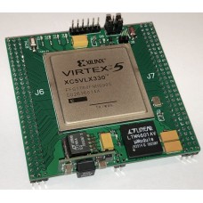
XILINX VIRTEX-5 XM3F5 FPGA module is designed for rapid prototyping and implementing FPGA designs. Board can be used for educational purposes. It can work independently or can be used as a control module in the bigger design.
Features
1) XILINX XC5VLX330 FPGA
• 51840 Virtex-5 Slices (331776 Logic Cells)
• 192x DSP48E Slices
• 288x 36Kb RAM blocks (10368Kb, 550MHz)
• 6 Clock Management Tiles
• 1200 User I/O (216 routed on this board)
2) INTEL JS28F128J3D-75 FLASH
• 128Mbit
• BPI Interface
• FPGA configuration
• Post-configuration access
• 100,000 erase cycles per block
3) Onboard IO peripherals
• 100MHz CMOS oscillator
• 4 LEDs
• 1 push button
4) Handy configuration
• Standard 2.54mm JTAG header
• Mode select jumpers
• DONE LED
• Push button for manual initiation of the configuration process
• Header for external reset
• Reset supervision by the voltage monitor
5) Onboard power supply
• 3.3V 8A (IO, PERIPHERALS)
• 2.5V 3A (VCCAUX)
• 1V 12A (CORE VOLTAGE)
• Input voltage range 11V – 13V
• POWER-GOOD LED
• J2 and J3 jumpers to use external I/O voltage 1.14V-3.45V
6) 168 independent I/O routed to the connectors
• J6 3x29 male pin connector (84 IO, 3 GND)
• J7 3x29 male pin connector (84 IO, 3 VCC)
• 2.54mm pitch for all connectors
• 1.14V-3.45V External I/O voltage can be used
• Small 74x74mm PCB designed to fit on the prototyping board with 2.54mm pitch
| FPGA / CPLD | |
| Equivalent Logic Cells | XC5VLX330 - 331776 |
| Block RAM Bits | XC5VLX330 - 10368 kb |
| Digital Clock Managers | 12 |
| Development board | |
| Crystal oscillator | 100 MHz CMOS |
| IO LEDs | 4 |
| IO push buttons | 1 |
| IO routed to connectors | 168 |
| FLASH | |
| Flash size | 128 Mbit |
| Flash type | BPI flash |


